What is Global Lead Frame for Semiconductor Market?
The Global Lead Frame for Semiconductor Market is a crucial aspect of the semiconductor industry. It is essentially a thin layer of metal that connects the wiring from tiny electrical terminals on the semiconductor surface to the large-scale circuitry on electrical devices and circuit boards. Lead frames are used in almost all semiconductor packages. Most kinds of integrated circuit packaging are made by placing the silicon chip on a lead frame, wire bonding the chip to the metal leads of that lead frame, and covering the chip with plastic. The metal leads protruding from the plastic are then either "cut long" and bent to form through-hole pins, or "cut short" and bent to form surface-mount leads. Such lead frames are used for surface mount packages with leads—such as Small-Outline Integrated Circuit (SOIC), Quad Flat Package (QFP), and Dual In-line Package (DIP).
Stamping Process Lead Frame, Etching Process Lead Frame, Others in the Global Lead Frame for Semiconductor Market:
The Global Lead Frame for Semiconductor Market is segmented into Stamping Process Lead Frame, Etching Process Lead Frame, and Others. The Stamping Process Lead Frame is a method where a machine press or stamping press uses a die to shape the lead frame. This process is usually used for high-volume production, as it is faster and more cost-effective. On the other hand, the Etching Process Lead Frame involves the use of chemicals to remove unwanted parts of the lead frame. This process is more precise and can create more complex shapes, but it is also more expensive and slower than the stamping process. The "Others" category includes various other methods used in the production of lead frames, such as casting or forging. Each of these methods has its own advantages and disadvantages, and the choice of method depends on the specific requirements of the semiconductor package.
Integrated Circuit, Discrete Device in the Global Lead Frame for Semiconductor Market:
The Global Lead Frame for Semiconductor Market finds its usage in various areas such as Integrated Circuit and Discrete Device. In the Integrated Circuit area, the lead frame is used as the foundation upon which circuits are constructed and electrically connected. It provides the electrical connection between the printed circuit board and the integrated circuit. In the Discrete Device area, the lead frame is used in the packaging of individual electronic components such as transistors and diodes. These devices are then used in a wide range of applications, from consumer electronics to industrial machinery. The use of lead frames in these areas is crucial for the functioning of these devices, as they provide the necessary electrical connections and help in heat dissipation.
Global Lead Frame for Semiconductor Market Outlook:
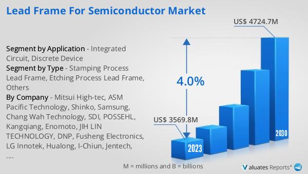
The Global Lead Frame for Semiconductor Market has shown significant growth in recent years. In 2022, the market was valued at US$ 3569.8 million. It is expected to grow at a steady pace, reaching a value of US$ 4724.7 million by 2029. This represents a Compound Annual Growth Rate (CAGR) of 4.0% during the forecast period from 2023 to 2029. This growth can be attributed to the increasing demand for semiconductors in various industries, including electronics, automotive, and telecommunications. The advancements in technology and the increasing need for miniaturization have also contributed to the growth of this market. However, the market also faces challenges such as the high cost of raw materials and the complex manufacturing process. Despite these challenges, the market is expected to continue its growth trajectory in the coming years.
| Report Metric | Details |
| Report Name | Lead Frame for Semiconductor Market |
| Accounted market size in 2022 | US$ 3569.8 million |
| Forecasted market size in 2029 | US$ 4724.7 million |
| CAGR | 4.0% |
| Base Year | 2022 |
| Forecasted years | 2023 - 2029 |
| Segment by Type |
|
| Segment by Application |
|
| Production by Region |
|
| Consumption by Region |
|
| By Company | Mitsui High-tec, ASM Pacific Technology, Shinko, Samsung, Chang Wah Technology, SDI, POSSEHL, Kangqiang, Enomoto, JIH LIN TECHNOLOGY, DNP, Fusheng Electronics, LG Innotek, Hualong, I-Chiun, Jentech, QPL Limited, Dynacraft Industries, Yonghong Technology, WuXi Micro Just-Tech |
| Forecast units | USD million in value |
| Report coverage | Revenue and volume forecast, company share, competitive landscape, growth factors and trends |


